Taiwan Semiconductor Manufacturing Co (TSMC, 台積電) on Saturday said that it would hold a ceremony on Thursday to mark the beginning of mass production using its 3-nanometer process.
The company is to mark the placing of the final beam at its Fab 18 in the Southern Taiwan Science Park (南部科學園區) in Tainan.
It would also detail its plans for expanding 3-nanometer production at the facility in the coming years, TSMC said.
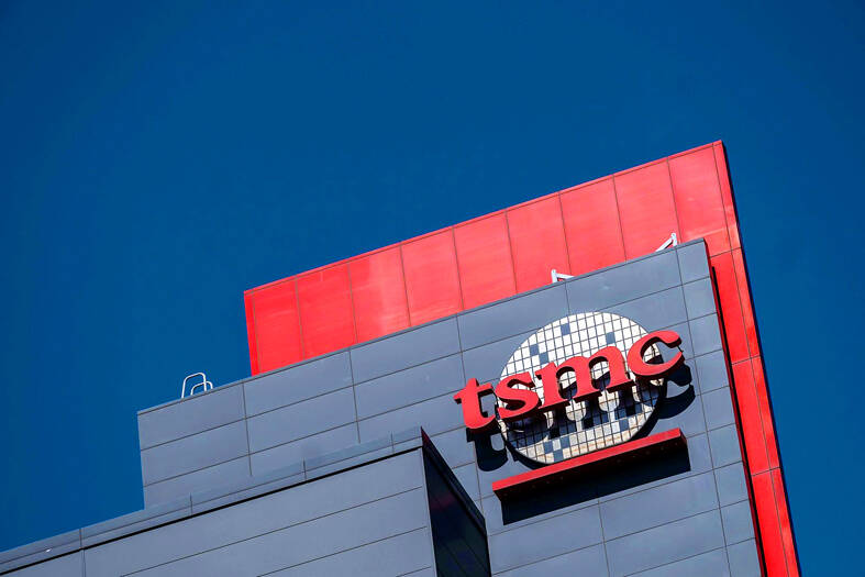
Photo: Lam Yik Fei, Bloomberg
The fab currently mass produces chips using the 5-nanometer process.
It is unusual for TSMC to hold a ceremony to mark the beginning of commercial production of a new technology.
Analysts have said that the ceremony aims to announce TSMC’s intention to continue using Taiwan as a hub for research and development (R&D) and production, despite its overseas investments.
Speculation has risen that the company could relocate its production and R&D centers to the US.
The rumors arose after TSMC on Dec. 6 said at a tool-in ceremony for its 12-inch wafer plant in Phoenix, Arizona, that it would increase its planned US$12 billion investment there to US$40 billion to build a 3-nanometer fab by 2026, in addition to its planned 4-nanometer plant due to be completed in 2024.
The concerns intensified after TSMC sent a large group of Taiwanese engineers to support the Arizona plant, raising investors’ fears that the move could undermine the firm’s base in Taiwan.
The planned Arizona plants are expected to produce more than 600,000 wafers a year, TSMC has said.
Last week, TSMC chief executive officer C.C. Wei (魏哲家) told a forum held by the Mount Jade Global Science and Technology Association in Taipei that there was “no chance” that a single wafer fab would give a location a technical advantage over other semiconductor manufacturing sites.
TSMC plans to start mass producing chips using the N3E process next year. The process is based on the 3-nanometer technology and produces more efficient chips with a better yield rate.
The company is also developing a more sophisticated 2-nanometer process and plans to build a 2-nanometer fab in Hsinchu, with mass production scheduled to begin in 2025.
The 3-nanometer process uses 16-nanometer fin field-effect transistor technology, which is a 3D transistor structure that allows a chip to run faster using the same amount of energy or to run at the same speed on reduced power.
Chips made using the technology are 10 to 15 percent faster and 25 to 30 percent more energy-efficient than those produced with the 5-nanometer process, whose mass production started last year.
Apple Inc and Intel Corp are expected to place orders for chips made with TSMC’s 3-nanometer process, analysts have said.
The 2-nanometer process would be the first technology in which TSMC employs a gate-all-around structure, which reduces undesirable variability and mobility loss, making the technology the most competitive and efficient on the market, the company has said.
Early this month, Wayne Wang (王永壯), director general of the Hsinchu Science Park Bureau, said TSMC has plans to build a 1-nanometer process fab in the Longtan (龍潭) section of the Hsinchu Science Park (新竹科學園區).
TSMC has yet to confirm Wang’s announcement.

Among the rows of vibrators, rubber torsos and leather harnesses at a Chinese sex toys exhibition in Shanghai this weekend, the beginnings of an artificial intelligence (AI)-driven shift in the industry quietly pulsed. China manufactures about 70 percent of the world’s sex toys, most of it the “hardware” on display at the fair — whether that be technicolor tentacled dildos or hyper-realistic personalized silicone dolls. Yet smart toys have been rising in popularity for some time. Many major European and US brands already offer tech-enhanced products that can enable long-distance love, monitor well-being and even bring people one step closer to

Malaysia’s leader yesterday announced plans to build a massive semiconductor design park, aiming to boost the Southeast Asian nation’s role in the global chip industry. A prominent player in the semiconductor industry for decades, Malaysia accounts for an estimated 13 percent of global back-end manufacturing, according to German tech giant Bosch. Now it wants to go beyond production and emerge as a chip design powerhouse too, Malaysian Prime Minister Anwar Ibrahim said. “I am pleased to announce the largest IC (integrated circuit) Design Park in Southeast Asia, that will house world-class anchor tenants and collaborate with global companies such as Arm [Holdings PLC],”

TRANSFORMATION: Taiwan is now home to the largest Google hardware research and development center outside of the US, thanks to the nation’s economic policies President Tsai Ing-wen (蔡英文) yesterday attended an event marking the opening of Google’s second hardware research and development (R&D) office in Taiwan, which was held at New Taipei City’s Banciao District (板橋). This signals Taiwan’s transformation into the world’s largest Google hardware research and development center outside of the US, validating the nation’s economic policy in the past eight years, she said. The “five plus two” innovative industries policy, “six core strategic industries” initiative and infrastructure projects have grown the national industry and established resilient supply chains that withstood the COVID-19 pandemic, Tsai said. Taiwan has improved investment conditions of the domestic economy

Sales in the retail, and food and beverage sectors last month continued to rise, increasing 0.7 percent and 13.6 percent respectively from a year earlier, setting record highs for the month of March, the Ministry of Economic Affairs said yesterday. Sales in the wholesale sector also grew last month by 4.6 annually, mainly due to the business opportunities for emerging applications related to artificial intelligence (AI) and high-performance computing technologies, the ministry said in a report. The ministry forecast that retail, and food and beverage sales this month would retain their growth momentum as the former would benefit from Tomb Sweeping Day